Automotive LED Driver Design: Good Practices to Ensure EMC Compliance

Get valuable resources straight to your inbox - sent out once per month
We value your privacy
March, 2020 -More and more automotive manufacturers are adopting LED lighting technology and moving away from halogen light bulbs. LED lighting systems have diverse power supply requirements, depending on the number of devices present on a string, the current needed, dimming, and other factors. A traditional linear regulator cannot always meet these needs. As a result, electronics engineers are increasingly relying on switch-mode power supplies (SMPS). However, SMPS create electromagnetic interference (EMI).
This article will discuss effective ways to improve the EMC of an LED driver design through component placement and layout, as well as features that semiconductor manufacturers are adding to their products.
PCB Layout
Mechanical dimensions and constraints (such as connector position and keep-out areas) are often placed such that engineers must work around them.
An effective way to ensure good EMC is to place the DC/DC converter far away from the connector and on the opposite side of the PCB, if two-sided assembly is possible. This minimizes noise coupling into the harness, which negates the effect of input filters. The input filter block should be placed close to the connector and away from the DC/DC, so that no noise is induced to the filter inductor.
If that is not possible, the designer should use a local shield for the DC/DC converter block (converter IC, inductor, and input capacitors). A shield adds cost to the design, but it can help save on filtering components, and it is often the difference between a design being compliant or not.
If the LED lighting solution requires a metallic heatsink for thermal dissipation, it can be used as a shield. There are two potential scenarios:
- The heatsink has several good connection points to GND that reduce emissions and protect the device from interference.
- The heatsink has a poor connection to GND (e.g. only one contact point), so the shielding is less effective, and may even act as a patch antenna. In this case, add a ferrite bead at the connection point between the heatsink and GND to improve the design’s immunity to interference.
When the LED load is not on the same PCB as the driver board, long load wires (>10cm) can create too much noise. To mitigate this, a common mode choke can be used at the input; however, a simpler solution is to place two ferrite beads at the VIN cable connection and the GND cable connection(see Figure 1).Use an output filter on both load cables to help with radiated emissions when conducted emissions are between 50MHz and 108MHz.
Making a Clever Layout
After planning PCB layout, consider where to route the DC/DC convert switch node.This articleoffers helpful instructions on how to design the DC/DC block.
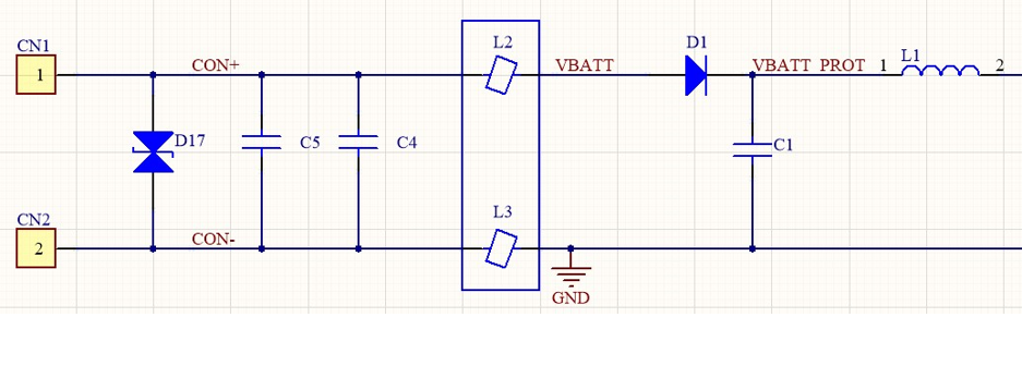
图1:好了Dri输入滤波器设计vers with Remote Loads
Automotive lighting is critical for safety, so it is important to maintain a low EMI on the LED driver circuit and a low susceptibility to interference. Compliant LED designs must maintain a certain level of brightness and stability regardless of perturbations.
Most LED driver ICs use a constant current approach, and may have current-sensing resistors. Other advanced drivers have several traces going into the IC that can pick up noise and potentially impact performance (e.g. temperature sensing or dimming).
路线这些痕迹的内部层board whenever possible, and shield them with copper on the external layers. When using a 2-layer PCB, route the traces by alternating between the top and bottom layers for short lengths. This method reduces the length of each trace, making the board immune to high-frequency interferences. It also avoids making a long cut to the GND plane on both layers. Cuts in the reference GND plane can add impedance and, depending on the size, create high-frequency noise.
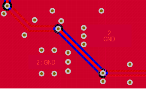
Figure 2: Routing a Long Trace in a 2-Layer Board
In small boards, where components are close with many traces, it is common to use vias for routing(see Figure 3).Ensure there is enough space that the GND copper plane can be placed between vias while avoiding big cuts. This is a common mistake in many layouts and is especially dangerous when a big cut is near the DC/DC block.
How Semiconductor Manufacturers are Improving the Technology
In recent years, semiconductor manufacturers have thought of ways to improve DC/DC power and efficiency while also improving the EMC of circuits.
Frequency spread-spectrum (FSS) modulation, sometimes called dithering, spreads the energy of the fundamental switching frequency on a wider band with a lower peak value. This allows the converter to pass EMC tests while switching inside the AM band. It also decreases noise radiated in the FM band when the converter switches above AM.
Another way to improve a converter’s EMI is to include an in-package decoupling capacitor. This reduces BOM cost and provides efficient decoupling by minimizing parasitic inductance between the capacitor and switches.
A good example of an advanced LED driver is MPS’sMPQ7200, which can operate as a buck converter or a buck-boost inverter (BBI). It is an AEC-Q100 qualified device that can supply a current of 3A when working in buck mode, and 1.2A when working in BBI mode, from a voltage up to 42V.
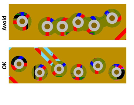
Figure 3: Connecting Different Layers with Vias
With a factory-trimmed FSS modulation option, the device offers improved EMI performance. It switches at 2.3MHz in buck mode, and at 1MHz in BBI mode. A low-loss current-sensing method is implemented in the silicon, eliminating the need for external current-sense resistors.
Typical buck-boost topology consists of four MOSFET switches, and the output voltage is positively referenced to GND. The MPQ7200’s BBI topology consists of only two MOSFET switches, which reduces costs and switching action. This two-switch BBI emulates buck topology, where the output side of the inductance is connected to ground. The control loop shifts the MPQ7200 power reference to a negative output voltage. The power LEDs can be connected between GND and the negative output voltage. In combination with the adjustable current control loop, temperature sensing, and digital dimming, the MPQ7200 is an advanced power LED driver.
Figure 4shows how theMPQ7200presents excellent line regulation over the typical operating voltages in an automotive application, with the input voltage varying from 15V to 10V, while the output voltage and current remain constant.
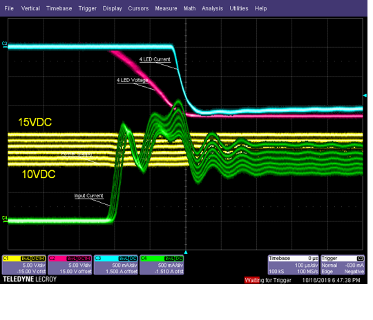
Figure 4: Start-Up Waveform of the MPQ7200
Another interesting test focuses on how input voltage interrupts affect the quality of the light beam. The input voltage interrupt sequence is the following: from 14VDC to 9.5V, to 8.5V, to 7.5V, to 6.5V, to 5.5V and to 4.5V. The low voltage valley time goes from 200ms rising up to 900ms. The visible light intensity remains almost constant down to low input voltages and at the 4.5V pulses the LED’s turned completely off.
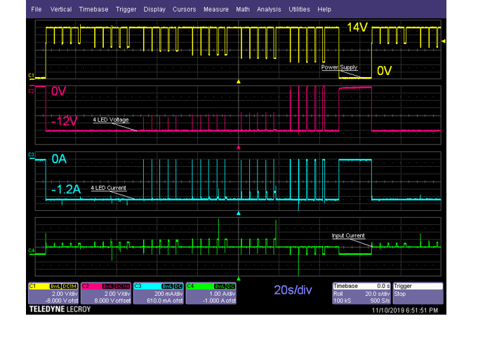
Figure 5: Power Supply Interrupt Test
Conclusion
LED技术允许在signallin创新g and safety, as more and more LEDs are used to help drivers communicate with their vehicles. Modern LED lighting designs need to offer great flexibility while remaining robust. This is possible thanks to functional improvements for LED drivers. Lighting solutions tend to be in small PCB with limited BOM count, so thoughtful component placement and layout design is necessary to meet increasing EMC requirements.
_________________________
Did you find this interesting?Get valuable resources straight to your inbox - sent out once per month!
Technical Forum
 Latest activity a week ago
 1 Comment
Latest activity 8 months ago
2 Comments
Latest activity 10 months ago
2 Comments
1 Comment
Latest activity 8 months ago
2 Comments
Latest activity 10 months ago
2 Comments
Log in to your account
Create New Account